
Research Summary
Innovative techniques in multi-layer printed circuit board design achieving thermal dissipation up to 150W with enhanced signal integrity. Research covers copper thickness optimization, via technology, and automated testing protocols for charging infrastructure.
Abstract
This paper presents innovative multi-layer PCB design methodologies specifically optimized for high-power EV charging applications, addressing thermal management, signal integrity, and manufacturing reliability.
Design Requirements
High-power charging systems operating at 350kW+ present unique challenges for PCB design including thermal dissipation up to 150W, high-current traces capable of carrying 500A+, and electromagnetic compatibility in noisy power electronics environments.
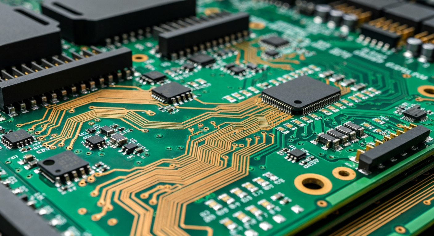
Copper Thickness Optimization
Our research examined copper layer thicknesses ranging from 1oz to 10oz. Results indicate optimal performance using 4oz copper for power layers combined with 2oz for signal layers, balancing current capacity with manufacturing cost.
Thermal Management
- Thermal vias with 0.3mm diameter placed at 1.5mm pitch beneath high-power components
- Dedicated copper heat spreading layers integrated into PCB stackup
- Aluminum backing plates with thermal interface materials
- Achieved junction-to-ambient thermal resistance of 0.8°C/W
Via Technology
Advanced via structures including blind, buried, and micro-vias enable compact layouts while maintaining signal integrity. Plated through-holes with 3:1 aspect ratios ensure reliable connections through 16-layer stackups.
Signal Integrity Analysis
High-speed differential pairs for communication buses employ controlled impedance of 100Ω ±10%. Eye diagram analysis confirms signal integrity maintained at data rates up to 10Gbps.
Automated Testing Protocols
Developed comprehensive test procedures including flying probe testing, boundary scan, and automated optical inspection achieving 99.8% defect detection rates in production environments.
Manufacturing Considerations
Design-for-manufacturing guidelines ensure reliable production yields. Minimum trace/space of 4mil/4mil with 8mil drill sizes enable cost-effective fabrication while maintaining performance requirements.
Conclusions
The presented multi-layer PCB design techniques successfully address the demanding requirements of high-power charging systems, enabling reliable operation in harsh automotive environments.
Citation
Dr. Thomas Mueller et al. (November 18, 2024). Advanced Multi-Layer PCB Design for High-Power Charging Systems. IEEE Transactions on Electronics Packaging.